- 您现在的位置:买卖IC网 > Sheet目录394 > AOK42S60L (Alpha & Omega Semiconductor Inc)MOSFET N-CH 600V 39A TO247
AOK42S60
General Description
600V 39A α MOS
Product Summary
TM
Power Transistor
The AOK42S60 has been fabricated using the advanced
α MOS TM high voltage process that is designed to deliver
high levels of performance and robustness in switching
applications.
By providing low R DS(on) , Q g and E OSS along with
guaranteed avalanche capability this device can be
V DS @ T j,max
I DM
R DS(ON),max
Q g,typ
E oss @ 400V
700V
166A
0.099 ?
40nC
9.2 μ J
adopted quickly into new and existing offline power supply
designs.
100% UIS Tested
100% R g Tested
For Halogen Free add "L" suffix to part number:
AOK42S60L
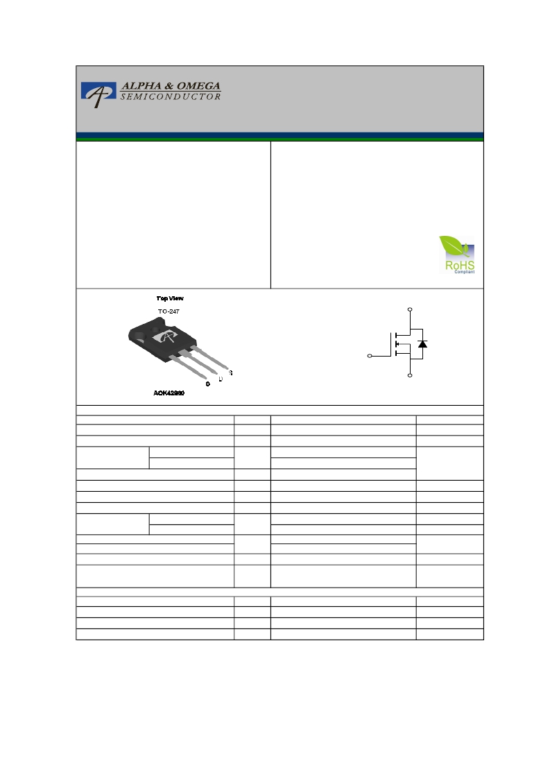
D
G
S
Absolute Maximum Ratings T A =25°C unless otherwise noted
Parameter
Drain-Source Voltage
Gate-Source Voltage
Symbol
V DS
V GS
AOK42S60
600
±30
Units
V
V
Continuous Drain
Current
Pulsed Drain Current C
T C =25°C
T C =100°C
I D
I DM
39
25
166
A
Avalanche Current C
Repetitive avalanche energy C
Single pulsed avalanche energy G
I AR
E AR
E AS
11
234
1345
A
mJ
mJ
Power Dissipation B
T C =25°C
Derate above 25 o C
P D
417
3.3
W
W/ o C
MOSFET dv/dt ruggedness
Peak diode recovery dv/dt H
Junction and Storage Temperature Range
dv/dt
T J , T STG
100
20
-55 to 150
V/ns
°C
Maximum lead temperature for soldering
purpose, 1/8" from case for 5 seconds J
T L
300
°C
Thermal Characteristics
Parameter
Maximum Junction-to-Ambient A,D
Maximum Case-to-sink A
Maximum Junction-to-Case
Rev0: Jan 2012
Symbol
R θ JA
R θ CS
R θ JC
www.aosmd.com
AOK42S60
40
0.5
0.3
Units
°C/W
°C/W
°C/W
Page 1 of 6
发布紧急采购,3分钟左右您将得到回复。
相关PDF资料
AON2405
MOSFET P CH 20V 8A DFN 2x2B
AON6232
MOSFET N CH 40V 85A DFN5X6
AON6244
MOSFET N CH 60V 85A DFN5X6
AON6918
MOSF 2N CH 25V 60/85A DFN5X6A
AON7421
MOSF P CH 20V 50A DFN3.3X3.3EP
AON7423
MOSF P CH 20V 50A DFN3.3X3.3EP
AON7426
MOSFET N-CH 30V 18A DFN3X3
AON7460
MOS N CH 300V 4A DFN3X3A_EP
相关代理商/技术参数
AOK50B60D1
制造商:Alpha & Omega Semiconductor 功能描述:IGBT 600V 100A 312W TO247
AOK50B60D1L
制造商:AOSMD 制造商全称:Alpha & Omega Semiconductors 功能描述:TO247 PACKAGE MARKING DESCRIPTION
AOK50B65H1
功能描述:IGBT 650V 50A TO-247 制造商:alpha & omega semiconductor inc. 系列:Alpha IGBT?? 零件状态:在售 IGBT 类型:- 电压 - 集射极击穿(最大值):650V 电流 - 集电极(Ic)(最大值):100A 脉冲电流 - 集电极 (Icm):150A 不同?Vge,Ic 时的?Vce(on):2.4V @ 15V,50A 功率 - 最大值:375W 开关能量:1.92mJ (开), 850μJ (关) 输入类型:标准 栅极电荷:76nC 25°C 时 Td(开/关)值:37ns/141ns 测试条件:400V,50A,6 欧姆,15V 反向恢复时间(trr):261ns 工作温度:-55°C ~ 175°C(TJ) 安装类型:通孔 封装/外壳:TO-247-3 供应商器件封装:TO-247 标准包装:240
AOK50B65M2
功能描述:IGBT 650V 50A TO247 制造商:alpha & omega semiconductor inc. 系列:Alpha IGBT?? 包装:管件 零件状态:有效 IGBT 类型:- 电压 - 集射极击穿(最大值):650V 电流 - 集电极(Ic)(最大值):100A 脉冲电流 - 集电极 (Icm):150A 不同?Vge,Ic 时的?Vce(on):2.2V @ 15V,50A 功率 - 最大值:500W 开关能量:2.09mJ(开),1.03mJ(关) 输入类型:标准 栅极电荷:102nC 25°C 时 Td(开/关)值:46ns/182ns 测试条件:400V,50A,6 欧姆,15V 反向恢复时间(trr):327ns 封装/外壳:TO-247-3 安装类型:通孔 供应商器件封装:TO-247 标准包装:240
AOK53S60
制造商:AOSMD 制造商全称:Alpha & Omega Semiconductors 功能描述:null600V 53A ?± MOS Power Transistor
AOK53S60L
制造商:Alpha & Omega Semiconductor 功能描述:MOSFET N-CH 600V 53A TO247
AOK5N100
制造商:Alpha & Omega Semiconductor 功能描述:MOSFET N-CH 1000V 4A TO247
AOK5N100L
制造商:Alpha & Omega Semiconductor 功能描述:MOSFET N-CH 1000V 4A TO247
